


 2020.02.27


Summary:The automatic sorting machine converts the image into a digital signal through the A/D converter, amplifies and processes the image, calculates the line marks, sorts the silicon wafers into the corresponding bins according to the weighed values, and sorts the silicon wafers into different grades. .
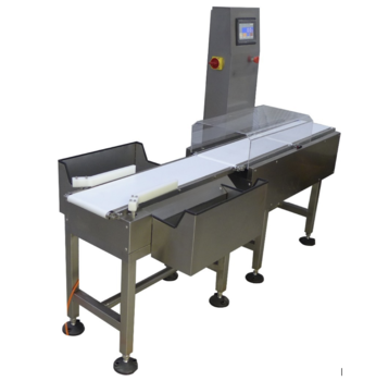
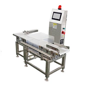
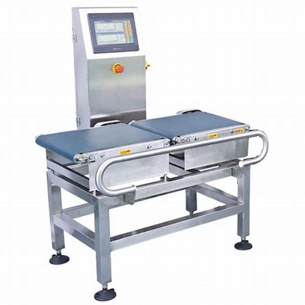
1 The basic composition of the weighing and testing machine is mainly composed of three parts: feeding table, weighing system and sorting system. Among them, the weighing system is the core part of the whole equipment, which contains the thickness module, line mark module, invisible crack module, dirty module, edge module and size, warpage module. When the wafers are fed from the loading table and pass through the weighing system, they will be detected and compared by these 6 modules to see if they meet the set requirements, and then sorted into the corresponding silos and boxes according to the weighed values, and finally the wafers will be sorted out into different grades.
2 The structure and working principle of each module of the weighing control system Here we briefly analyze the structure and working principle of each module. Thickness detection module, also known as E+H thickness measurement module, its working principle is to use capacitive coupling method to weigh the thickness of silicon wafers. There are three pairs of sensors on the module, each with two capacitive sensors above and below, which generate different voltage values according to the distance from the wafer (Ttop, Tbottom), and the distance is generally proportional to the voltage. The voltage signals are analog and are converted to digital signals by an A/D converter. The distance between the top and bottom sensors is a fixed value Ttotal, so the thickness of the wafer T = Ttotal - (Ttop + Tbottom). When the wafer passes through the sensors, the thickness is normally detected at about 900 points. Then the average thickness and TTV i.e. thickness deviation is calculated. So the detected thickness value is very much. The line trace detection module is used to detect the flatness of the wafer surface, which mainly consists of 4 lenses and 4 laser emitters. It is used to incident the laser to the wafer surface at 14°. The matrix camera takes a total of 11 pictures during the wafer transfer process and analyzes the pictures. The surface of the wafer is high and low, and under the red laser line at a fixed angle, it will show a high and low image. The images are enlarged and processed to calculate the line marks. There are generally 3 types of expressions: V-shaped notch type, step type and gentle wave type. The invisible crack detection module, referred to as NVCD detection module, is a module that detects invisible cracks (also known as microcracks, microcracks) in silicon wafers using a linear camera and an infrared light source. The module can also detect impurities (inclusion). In normal areas, infrared light will pass through the wafer, but because of the different crystal orientations (grains), it will show a different color (appear as scattered light) in the image, which is essentially the same as the appearance of the wafer as viewed by the naked eye. If the wafer is cracked, when the infrared ray is irradiated, the infrared light will not be transmitted in the cracked area, but will be largely reflected in all directions, thus making the cracked area appear black. The dirt detection module is a linear camera using an array of white LEDs. The silicon wafer is divided into a number of blocks, each block has 20 basic pixels (adjustable, each pixel size is about 100um), each block separately calculates its own internal average gray scale (RGBvalue) and compares it with the other 8 adjacent blocks, if the difference in gray scale is greater than 15 (adjustable), it is recognized that the block is a stained block.The LED arrays emit a very high intensity of white light, which after being The white light from the LED arrays, after being reflected by the mask, is directed to each area of the wafer surface at a full angle, so that each grain is irradiated by the light in all directions, and will not produce a difference in grayscale because of its own different crystal directions. The edge detection module has a LineCamera and a red light source on the top and bottom. The LineCamera takes 2000 shots/second, and each shot of the wafer is a long strip, which is stitched together to form the Edge detection image of the wafer. And by analyzing the RGB values (grayscale, gray scale) of different pixel (pixel) and the RGB values between pixels, Chip, Breakage, Holes, Cracks are judged. size, warpage detection module is mainly composed of 1 lens, 2 LED red light sources and 2 laser emitters. When detecting BOW/SORI (two forms of warpage), 2 laser lines (diffracted with a grating to a length of 160mm or more) are used, which are incident on the wafer at 9° (the laser is parallel to the wafer's direction of travel), and are detected by casting a laser beam on the wafer.
3 weighing sorting machine common faults and solutions When the equipment fails, we can view the current error messages in the "Errors" window, you can view all the confirmed and unrecognized in the "Protocol" window. These messages are listed in chronological order.
3.1 High Thickness Part Value (TTV): Fragmentation of the wafer left on the thickness sensor; defects in the electrical system; defects in the wiring. Low value (TTV): wrong position of the outer sensor TTV value shows 0: power supply is switched off.
3.2 The white laser image cannot be observed in the software window in the line trace section: If the equipment is being serviced, make sure that the power has been turned off, e.g., the red emergency stop button has been pressed; check the software settings; the motor controlling the width between the cameras has been moved to the wrong position; check that the lasers are working properly; check the status of the power supply to the lasers; check that the camera functions properly; check that the data cable connecting the camera to the computer is not damaged; check the internal computer cable for damage; check the laser image. Data cable is not damaged; check whether the internal FireWire adapter of the computer is working properly. The edge of the wafer is not visible: check the speed setting of the conveyor system; the weighing value of the line trace is high; the camera lens is not focused accurately; the weighing position of the laser on the wafer is too close to the edge.
3.3 Dirty parts cannot be observed as images in the software: Check the light source. Consistently poor quality: Brightness of the light source is dark; wrong camera settings (e.g. focus); wrong wafer position; wafer crumbles on the camera lens below. 3.4 Warpage/geometry part of the image cannot be observed in the software: Check that the LED light source is working correctly. Consistently poor quality: light source too dark; wrong camera settings (e.g. focusing); wrong wafer position.
4 Conclusion
The electronic technology possessed by the checkweigher utilizes the imaging principle of the camera, laser, infrared, and the application of capacitive coupling to accurately weigh out the wafer's thickness, surface flatness, dirtiness, size, verticality, and so on, which improves the efficiency of detecting the quality of silicon wafers. Weighing system is the core part of the weighing sorting machine, only familiar with its working principle in order to make accurate judgment on the equipment failure, in order to carry out better maintenance and repair, to ensure the stable operation of the equipment.